OSAKA, Japan & KAWASAKI, Japan--(BUSINESS WIRE)--Panasonic Corporation (Panasonic) and Institute of Microchemical Technology Co., Ltd. (IMT) jointly developed a technology for mass production of microfluidic devices*2 using a glass molding. Compared to the conventional glass etching method, this technology realizes low cost (about 1/10) and highly accurate (about 10 times) mass production. These devices can be applied to sensing and analysis for medical, biological, environmental (water and air quality) applications, etc. The companies will start accepting prototype orders from FY2019, and are planning to start mass production from FY2020. Panasonic and IMT will present and exhibit this device at the 40th meeting of Society for Chemistry and Micro-Nano Systems (CHEMINAS 40th) held at Act City Hamamatsu in Hamamatsu City, Shizuoka Prefecture, Japan from November 19th to 21st.
[Effect]
Conventional glass microfluidic devices have not been widely used, because of high cost and poor precision. This development achieved mass production and cost reduction of glass microfluidic devices by combining IMT's microfluidic device design technology and Panasonic's glass molding technology. As a result, disposable use of glass microfluidic devices becomes possible. In addition, by realizing high precision, it is easy to incorporate the device as a part of equipment and systems.
[Application]
By taking advantage of the environmental and chemical resistance of glass microfluidic devices, it can be applied to environmental sensing, blood testing, and pharmaceutical equipment as disposable detection devices for analysis and testing in outdoor and harsh environments.
[Characteristic]
The newly developed microfluidic device has the following features.
1. Up to φ50mm size
2. More than 10,000 devices per month of production capacity
3. Manufacturing process with the shape precision of about 1μm
[Technology]
This development is realized by the following technologies.
(1) Design and interface technology of microfluidic device optimized for glass molding
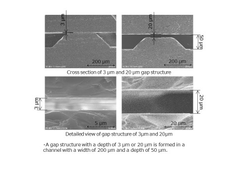
(2) Microstructure mold processing technology to higher hardness material and microstructural glass molding technology to precisely transfer to glass
(3) Thermal bonding technology to join a flat glass plate and a plate with microstructures.
Notes:
*1: As of November 6, 2019, Panasonic survey
*2: A device that can perform various chemical processes (mixing, reaction, extraction, synthesis, detection) in a minute flow path with a small amount and high efficiency by flowing liquid through a groove with a width and depth of several hundreds of micrometers.
[Background]
General microfluidic device made of glass used in microfluidics technology [1] is mainly produced by etching techniques. After drawing the flow path pattern by photolithography, the glass flow path is formed by etching, and the cover glass with the machined introduction hole is bonded. Since the inception of this field, IMT has provided high-level products as a pioneer in the planning, design and manufacture of glass microfluidic devices. However, in addition to the skill required for manual manufacturing, the manufacturing process took several months. For this reason, the manufacturing time and cost per piece became a hurdle, and generalization and industrial mounting were not realized, and the use was limited mainly to basic research applications.
On the other hand, Panasonic has been developing and manufacturing glass molding technology [2] from the 1980s, that has contributed to the commercialization of the world's highest level of optical device. They are used in lenses for various optical devices, like digital still cameras.
By combining Panasonic's glass molding technology and IMT design technology, it became possible to develop microstructure mold machining technology, molding technology, and joining technology suitable for mass production of microfluidic devices using glass molding technology. The companies have succeeded in developing mass production technology for microfluidic devices. As a result, it is possible to reduce the cost to about 1/10 compared to the conventional manufacturing method, and to supply glass microfluidic devices with improved precision 10 times or more in less than half the delivery time.
[Practical realization]
With the development of mass production technology for microfluidic devices [3] using this glass molding technology, glass microfluidic devices are widely used as disposable detection devices for analysis and testing in outdoor and harsh environments, and for disposable devices for blood testing equipment.
[Explanation of terms]
[1] Microfluidic device technology
This technology integrates chemical processes such as mixing, reaction, separation, extraction, synthesis, and detection in a flow channel of several tens to several hundreds of μm created on a substrate (microfluidic device) of several cm square. By freely integrating chemical processes that have been performed in laboratories and factories in the microspace of microfluidic devices, it becomes possible to use energy and space much more efficiently. It is expected to contribute greatly to the evolution of chemical technology in the future. This chemical process integration technology (microfluidic technology) in the micro space was established as a result of research and development of the Kitamori “Integrated Chemistry” project. The project was carried out at Kitamori Lab., Department of Applied Chemistry, School of Engineering, The University of Tokyo, and Kanagawa Academy of Science and Technology (currently Kanagawa Institute of Industrial Science and Technology).
[2] Glass molding technology (mold machining technology, mold protection coating technology, molding technology)
[3] Application examples of microfluidic devices using glass molding technology
About Panasonic
Panasonic Corporation is a worldwide leader in the development of diverse electronics technologies and solutions for customers in the consumer electronics, housing, automotive, and B2B businesses. The company, which celebrated its 100th anniversary in 2018, has expanded globally and now operates 582 subsidiaries and 87 associated companies worldwide, recording consolidated net sales of 8.003 trillion yen for the year ended March 31, 2019. Committed to pursuing new value through innovation across divisional lines, the company uses its technologies to create a better life and a better world for its customers. To learn more about Panasonic: https://www.panasonic.com/global.
About Institute of Microchemical Technology
IMT is a pioneer company of microchemical chip technology (microfluidics) and was founded in 2001 as a venture company of the University of Tokyo and Kanagawa Institute of Industrial Science and Technology (formerly Kanagawa Academy of Science and Technology).
IMT manufactures and sells microchemical chips, their peripheral equipment and system devices.
Company Name: Institute of Microchemical Technology Co., Ltd (IMT)
Capital: 100M JPY
Foundation: May 1st, 2001
Address: A-19 AIRBIC, 7-7 Shinkawasaki, Saiwai, Kawasaki, Kanagawa 212-0032 Japan
TEL: +81-44-201-9889 FAX: +81-44-201-9890
HP: https://www.i-mt.co.jp/en/
Source: https://news.panasonic.com/global/press/data/2019/11/en191106-3/en191106-3.html
Related Links
Industrial Devices & Solutions - Panasonic
https://industrial.panasonic.com/ww
Contacts
Panasonic
Innovation Strategy Office
Technology Public Relations Section
crdpress@ml.jp.panasonic.com
[Inquiries for prototypes]
Institute of Microchemical Technology Co., Ltd.
Email:info@i-mt.co.jp Tel: +81-44-201-9889
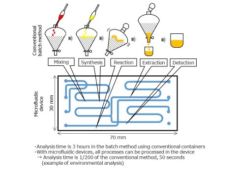
Microfluidic device technology (Graphic: Business Wire)
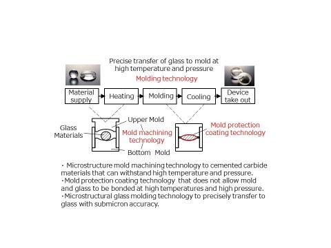
Glass molding technology (mold machining technology, mold protection coating technology, molding technology) (Graphic: Business Wire)
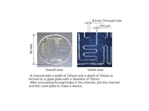
Application example 1: Water quality inspection device (Graphic: Business Wire)
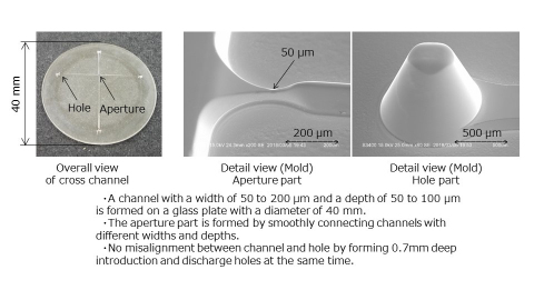
Application example 2: General-purpose device (Graphic: Business Wire)
Application Example 3: Genetic testing device (Graphic: Business Wire)


